2020
|
T D Bucio, C Lacava, M Clementi, J Faneca, I Skandalos, A Baldycheva, M Galli, K Debnath, P Petropoulos, F Gardes Silicon Nitride Photonics for the Near-Infrared Journal Article IEEE Journal of Selected Topics in Quantum Electronics, 26 (2), 2020. Abstract | Links | Tags: silicon nitride, Silicon photonics, silicon-rich @article{Bucio2020,
title = {Silicon Nitride Photonics for the Near-Infrared},
author = {T D Bucio and C Lacava and M Clementi and J Faneca and I Skandalos and A Baldycheva and M Galli and K Debnath and P Petropoulos and F Gardes},
doi = {10.1109/JSTQE.2019.2934127},
year = {2020},
date = {2020-01-01},
journal = {IEEE Journal of Selected Topics in Quantum Electronics},
volume = {26},
number = {2},
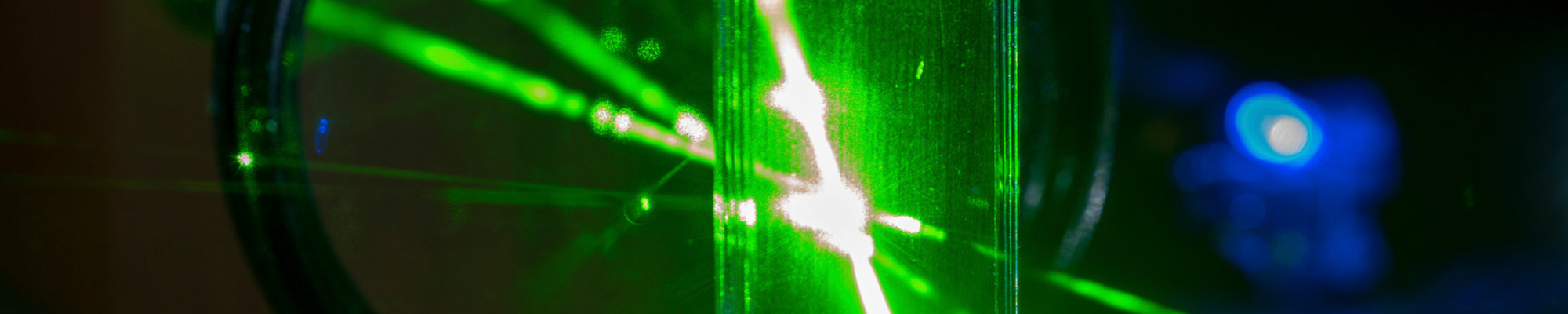
abstract = {In recent years, silicon nitride (SiN) has drawn attention for the realisation of integrated photonic devices due to its fabrication flexibility and advantageous intrinsic properties that can be tailored to fulfill the requirements of different linear and non-linear photonic applications. This paper focuses on our progress in the demonstration of enhanced functionalities in the near infrared wavelength regime with our low temperature (textless350 ^$backslash$circC) SiN platform. It discusses (de)multiplexing devices, nonlinear all optical conversion, photonic crystal structures, the integration with novel phase change materials, and introduces applications in the 2 $backslash$mum wavelength range.},
keywords = {silicon nitride, Silicon photonics, silicon-rich},
pubstate = {published},
tppubtype = {article}
}
In recent years, silicon nitride (SiN) has drawn attention for the realisation of integrated photonic devices due to its fabrication flexibility and advantageous intrinsic properties that can be tailored to fulfill the requirements of different linear and non-linear photonic applications. This paper focuses on our progress in the demonstration of enhanced functionalities in the near infrared wavelength regime with our low temperature (textless350 ^$backslash$circC) SiN platform. It discusses (de)multiplexing devices, nonlinear all optical conversion, photonic crystal structures, the integration with novel phase change materials, and introduces applications in the 2 $backslash$mum wavelength range. |
2019
|
C Lacava, M A Ettabib, T D Bucio, G Sharp, A Z Khokhar, Y Jung, M Sorel, F Gardes, D J Richardson, P Petropoulos, P Petropoulos, F Parmigiani Intermodal bragg-scattering four wave mixing in silicon waveguides Journal Article Journal of Lightwave Technology, 37 (7), pp. 1680–1685, 2019. Abstract | Links | Tags: frequency generation, intermodal, intermodal four wave mixing, silicon, Silicon photonics, silicon-rich, wavelength conversion, wavelength converter @article{Lacava2019,
title = {Intermodal bragg-scattering four wave mixing in silicon waveguides},
author = {C Lacava and M A Ettabib and T D Bucio and G Sharp and A Z Khokhar and Y Jung and M Sorel and F Gardes and D J Richardson and P Petropoulos and P Petropoulos and F Parmigiani},
doi = {10.1109/JLT.2019.2901401},
year = {2019},
date = {2019-01-01},
journal = {Journal of Lightwave Technology},
volume = {37},
number = {7},
pages = {1680--1685},
abstract = {We demonstrate optical wavelength conversion in a multi-mode silicon waveguide using four wave mixing Bragg scattering enabled by a dual-pump CW scheme. The original signal and the generated idler pair excite one spatial mode (first, TE mode), while the two pumps excite a different spatial mode (second, TE mode) of the same waveguide. Our approach exploits the differences in the group velocities of the various supported spatial modes to ensure phase matching only for the desired nonlinear process. In this proof-of-principle experiment, any unintended idlers are generated with an extinction ratio up to 12 dB relative to the phase-matched idlers for a pumps-to-signal-idler-pair wavelength detuning of about 70 nm. The scalability of the scheme to achieve larger and multiple signal wavelength detunings from the pump frequencies is also discussed.},
keywords = {frequency generation, intermodal, intermodal four wave mixing, silicon, Silicon photonics, silicon-rich, wavelength conversion, wavelength converter},
pubstate = {published},
tppubtype = {article}
}
We demonstrate optical wavelength conversion in a multi-mode silicon waveguide using four wave mixing Bragg scattering enabled by a dual-pump CW scheme. The original signal and the generated idler pair excite one spatial mode (first, TE mode), while the two pumps excite a different spatial mode (second, TE mode) of the same waveguide. Our approach exploits the differences in the group velocities of the various supported spatial modes to ensure phase matching only for the desired nonlinear process. In this proof-of-principle experiment, any unintended idlers are generated with an extinction ratio up to 12 dB relative to the phase-matched idlers for a pumps-to-signal-idler-pair wavelength detuning of about 70 nm. The scalability of the scheme to achieve larger and multiple signal wavelength detunings from the pump frequencies is also discussed. |
2017
|
T Domínguez Bucio, A Z Khokhar, C Lacava, S Stankovic, G Z Mashanovich, P Petropoulos, F Y Gardes Material and optical properties of low-temperature NH3-free PECVD SiNx layers for photonic applications Journal Article Journal of Physics D: Applied Physics, 50 (2), 2017. Abstract | Links | Tags: nonlinear optics, nonlinear waveguides, silicon nitride, Silicon photonics, silicon-rich @article{DominguezBucio2017,
title = {Material and optical properties of low-temperature NH3-free PECVD SiNx layers for photonic applications},
author = {T {Domínguez Bucio} and A Z Khokhar and C Lacava and S Stankovic and G Z Mashanovich and P Petropoulos and F Y Gardes},
doi = {10.1088/1361-6463/50/2/025106},
year = {2017},
date = {2017-01-01},
journal = {Journal of Physics D: Applied Physics},
volume = {50},
number = {2},
abstract = {SiNx layers intended for photonic applications are typically fabricated using LPCVD and PECVD. These techniques rely on high-temperature processing (textgreater400 °C) to obtain low propagation losses. An alternative version of PECVD SiNx layers deposited at temperatures below 400 °C with a recipe that does not use ammonia (NH3-free PECVD) was previously demonstrated to be a good option to fabricate strip waveguides with propagation losses textless3 dB cm-1. We have conducted a systematic investigation of the influence of the deposition parameters on the material and optical properties of NH3-free PECVD SiNx layers fabricated at 350 °C using a design of experiments methodology. In particular, this paper discusses the effect of the SiH4 flow, RF power, chamber pressure and substrate on the structure, uniformity, roughness, deposition rate, refractive index, chemical composition, bond structure and H content of NH3-free PECVD SiNx layers. The results show that the properties and the propagation losses of the studied SiNx layers depend entirely on their compositional N/Si ratio, which is in fact the only parameter that can be directly tuned using the deposition parameters along with the film uniformity and deposition rate. These observations provide the means to optimise the propagation losses of the layers for photonic applications through the deposition parameters. In fact, we have been able to fabricate SiNx waveguides with H content textless20%, good uniformity and propagation losses of 1.5 dB cm-1 at 1550 nm and textless1 dB cm-1 at 1310 nm. As a result, this study can potentially help optimise the properties of the studied SiNx layers for different applications.},
keywords = {nonlinear optics, nonlinear waveguides, silicon nitride, Silicon photonics, silicon-rich},
pubstate = {published},
tppubtype = {article}
}
SiNx layers intended for photonic applications are typically fabricated using LPCVD and PECVD. These techniques rely on high-temperature processing (textgreater400 °C) to obtain low propagation losses. An alternative version of PECVD SiNx layers deposited at temperatures below 400 °C with a recipe that does not use ammonia (NH3-free PECVD) was previously demonstrated to be a good option to fabricate strip waveguides with propagation losses textless3 dB cm-1. We have conducted a systematic investigation of the influence of the deposition parameters on the material and optical properties of NH3-free PECVD SiNx layers fabricated at 350 °C using a design of experiments methodology. In particular, this paper discusses the effect of the SiH4 flow, RF power, chamber pressure and substrate on the structure, uniformity, roughness, deposition rate, refractive index, chemical composition, bond structure and H content of NH3-free PECVD SiNx layers. The results show that the properties and the propagation losses of the studied SiNx layers depend entirely on their compositional N/Si ratio, which is in fact the only parameter that can be directly tuned using the deposition parameters along with the film uniformity and deposition rate. These observations provide the means to optimise the propagation losses of the layers for photonic applications through the deposition parameters. In fact, we have been able to fabricate SiNx waveguides with H content textless20%, good uniformity and propagation losses of 1.5 dB cm-1 at 1550 nm and textless1 dB cm-1 at 1310 nm. As a result, this study can potentially help optimise the properties of the studied SiNx layers for different applications. |
C Lacava, S Stankovic, A Khokhar, T Bucio, F Gardes, G Reed, D Richardson, P Petropoulos Si-rich Silicon Nitride for Nonlinear Signal Processing Applications Journal Article Scientific Reports, 7 (1), 2017. Abstract | Links | Tags: nonlinear optics, silicon nitride, Silicon photonics, silicon-rich @article{Lacava2017,
title = {Si-rich Silicon Nitride for Nonlinear Signal Processing Applications},
author = {C Lacava and S Stankovic and A Khokhar and T Bucio and F Gardes and G Reed and D Richardson and P Petropoulos},
doi = {10.1038/s41598-017-00062-6},
year = {2017},
date = {2017-01-01},
journal = {Scientific Reports},
volume = {7},
number = {1},
abstract = {Nonlinear silicon photonic devices have attracted considerable attention thanks to their ability to show large third-order nonlinear effects at moderate power levels allowing for all-optical signal processing functionalities in miniaturized components. Although significant efforts have been made and many nonlinear optical functions have already been demonstrated in this platform, the performance of nonlinear silicon photonic devices remains fundamentally limited at the telecom wavelength region due to the two photon absorption (TPA) and related effects. In this work, we propose an alternative CMOS-compatible platform, based on silicon-rich silicon nitride that can overcome this limitation. By carefully selecting the material deposition parameters, we show that both of the device linear and nonlinear properties can be tuned in order to exhibit the desired behaviour at the selected wavelength region. A rigorous and systematic fabrication and characterization campaign of different material compositions is presented, enabling us to demonstrate TPA-free CMOS-compatible waveguides with low linear loss (∼1.5 dB/cm) and enhanced Kerr nonlinear response (Re$gamma$ = 16 Wm-1). Thanks to these properties, our nonlinear waveguides are able to produce a $pi$ nonlinear phase shift, paving the way for the development of practical devices for future optical communication applications.},
keywords = {nonlinear optics, silicon nitride, Silicon photonics, silicon-rich},
pubstate = {published},
tppubtype = {article}
}
Nonlinear silicon photonic devices have attracted considerable attention thanks to their ability to show large third-order nonlinear effects at moderate power levels allowing for all-optical signal processing functionalities in miniaturized components. Although significant efforts have been made and many nonlinear optical functions have already been demonstrated in this platform, the performance of nonlinear silicon photonic devices remains fundamentally limited at the telecom wavelength region due to the two photon absorption (TPA) and related effects. In this work, we propose an alternative CMOS-compatible platform, based on silicon-rich silicon nitride that can overcome this limitation. By carefully selecting the material deposition parameters, we show that both of the device linear and nonlinear properties can be tuned in order to exhibit the desired behaviour at the selected wavelength region. A rigorous and systematic fabrication and characterization campaign of different material compositions is presented, enabling us to demonstrate TPA-free CMOS-compatible waveguides with low linear loss (∼1.5 dB/cm) and enhanced Kerr nonlinear response (Re$gamma$ = 16 Wm-1). Thanks to these properties, our nonlinear waveguides are able to produce a $pi$ nonlinear phase shift, paving the way for the development of practical devices for future optical communication applications. |